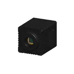
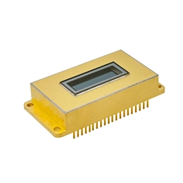
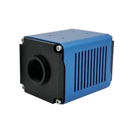
Today, the semiconductor industry has grown into one of the largest industries in the world, and its growth shows no signs of slowing down. Wafer integrated circuit production is the focus of this industry. Short wave infrared imaging with sensors can achieve spectral imaging of wavelengths through semiconductor materials, and has become an essential device for the inspection process. Transparent imaging of silicon wafers is a non-destructive testing method that provides many benefits to the production process. Now, the semiconductor industry is incorporating cameras into testing, inspection, and quality control systems.
Inspection of silicon crystals and ingots (also known as bricks) is one of the typical applications of cameras in the semiconductor industry. Short wave infrared imaging can achieve imaging of the spectral transmission of silicon-based materials, and is an ideal solution for detecting impurities that may accumulate in crystals or rods during the production process. The crystal rods need to be cut into wafer-thin slices using special diamond cutting tools, and the purity of the wafers is crucial during this process. Even if there is only a small piece of metal impurity in the wafer, it may cause the expensive diamond cutting tool to break and be scrapped. Replacing tools not only incurs costs, but also leads to a decrease in production efficiency and profits. The introduction of shortwave infrared cameras can avoid this problem and ensure the smooth progress of the production process.
Another important application of short wave infrared imaging is wafer inspection. During the wafer production process, particles may appear on the top, bottom, or even inside or between the wafers. CCD or CMOS cameras can detect particles on the top and bottom, while cameras can detect particles between two bonded wafers through silicon-based materials. Cameras can also be used for wafer packaging, i.e., detecting whether the arrangement on the back of the wafer is aligned with the front. Shortwave infrared technology can help align various layers of wafers and align the wafer substrate and other sub-products, such as ICs, memory units, or transistors.
From silicon crystals to ingots/bricks, wafers, solar cells, and even solar modules, swir infrared camera applications can cover the entire photovoltaic power generation supply chain inspection process. As it can achieve transparent imaging of silicon-based materials, it is a very effective solution for detecting physical defects inside silicon-based materials. In addition to the newly emerging shortwave infrared imaging inspection technology, other important technologies and methods commonly used in the photovoltaic industry include photoluminescence and electroluminescence.
Compared with CCD and CMOS cameras, the main advantage of shortwave infrared is that it has a shorter exposure time and excellent quantum efficiency in its main emission wavelength range, ensuring quick identification in the production process. CCD or CMOS cameras require longer exposure times, up to 30 seconds. Even NIR-enhanced CCD sensors require exposure times of 3 seconds or more. Shortwave infrared cameras only require a few milliseconds, significantly increasing production capacity.


