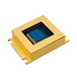
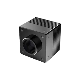
An image sensor, also known as a photosensitive element, is a device that converts optical images into electronic signals. It is widely used in digital cameras and other electronic optical devices. Early image sensors used analog signals, such as camera tubes. This image sensor definition encompasses both historical analog designs and modern digital implementations.
With the rapid development of digital technology, semiconductor manufacturing technology, and networks, the market and industry are facing the arrival of an era of cross-platform integration of video, audio, and communication. Image sensing technology has also made greater advances. In recent years, with the rise of artificial intelligence, as one of the input signals, image sensors support many important applications such as face detection, industrial anomaly detection, and gesture recognition. To understand the role they play, it’s essential to know the image sensor definition: an image sensor is a device that converts an optical image into an electronic signal, enabling the capture and processing of visual information in various applications.
CCD is a high-end technology element applied in photography and video, while CMOS is applied in products with lower image quality. Its advantages are lower manufacturing costs and much lower power consumption, which is why many products that use USB interfaces do not require external power sources and are cheap. CIS is a contact image sensing device. It uses a contact-sensitive element for sensing, and scanners made using CIS technology have many advantages such as small size, light weight, and low production cost, and are widely used in fields such as fax machines, scanners, and bill sorting. However, CIS technology also has its shortcomings, such as unable to make high-resolution scanners and slower scanning speeds, so CCD and CMOS are the two main image sensor devices widely used in the market.
Although there are significant differences in technology, the performance gap between CCD and CMOS is not very large. Both are fundamental technologies within the broad image sensor definition, which encompasses devices that convert light into electrical signals. CCD can be divided into linear and planar types, with linear types used in imaging scanners and fax machines, while planar types are mainly used in many image input products such as digital cameras, camcorders, and surveillance cameras. Understanding the image sensor definition helps clarify why CCD sensors have the advantages of high resolution, low noise, wide dynamic range, good linear characteristics, high photon conversion efficiency, large area photosensitivity, wide spectral response, low image distortion, small size, light weight, low power consumption, good charge transfer efficiency, immunity to strong electromagnetic fields, and can be mass-produced.
Compared with CCD, CMOS sensors use the most commonly used CMOS process for general semiconductor circuits and have advantages such as high integration, low power consumption, fast speed, and low cost. In recent years, they have developed rapidly in wide dynamic range and low light. CMOS mainly uses silicon and germanium to make semiconductors and uses transistors with negative and positive charges on CMOS to achieve basic functions. The current generated by the two complementary effects can be recorded and interpreted as images by the processing chip.
Since the 1990s, CMOS image sensor technology has been highly regarded in the industry and has received a lot of research and development resources, continuously squeezing the market space of CCD image sensors. CMOS image sensor chips have become an important component of global integrated circuits, and their main advantages can be summarized as three levels:
In terms of cost: CMOS image sensor chips generally use standard process technology suitable for mass production, and their unit cost is far lower than that of CCD in mass production;
In terms of size: CMOS sensors can concentrate image capture units and signal processing units on the same substrate, greatly reducing the volume, making them very suitable for mobile devices and various miniaturized devices;
In terms of power consumption: CMOS sensors still maintain the advantages of low power consumption and low heat generation compared to CCD.


