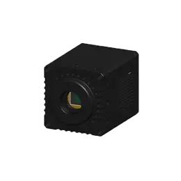
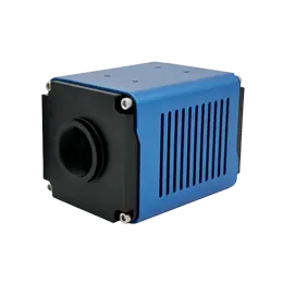
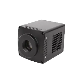
The semiconductor industry has become one of the largest industries in the world. The semiconductor industry covers a wide range of applications, from PCs to processors and memories for mobile devices, from integrated circuits to solar cells.
In the semiconductor industry, short-wave ir cameras can be used to detect the quality of pure semiconductor materials (usually the growth of silicon ingots). In addition, silicon ingots and finished wafers cut into wafers can also be tested for defects or cracks in a similar way. The wafer is then processed into optoelectronic components or other semiconductor devices. In the process of finally cutting the wafer into a single chip, short-wave ir cameras are still the mainstream solution currently used for saw blades and laser calibration.
To perform failure analysis, the assembled integrated circuit must be inspected for cracks or photolithography. For example, MEMS (Micro Electro Mechanical System) requires testing throughout the production process. In these applications, short wave ir camera is indispensable. The short wave IR cameras used usually use indium gallium arsenide (InGaAs) detectors, which can have high responsivity and high quantum efficiency in the 900~1700nm band, so they are very suitable for silicon surface or internal imaging.
Using short wave ir camera imaging to detect defects in semiconductor wafers and integrated circuit chips will achieve a multiplier effect with half the effort. Si material is currently the most commonly used for infrared semiconductor inspection, and InGaAs sensor can detect short-wave infrared bands passing through Si material. Therefore, the InGaAs short wave ir camera provides a non-destructive inspection method for semiconductor inspection, which greatly improves the inspection efficiency and improves the production process.
During the wafer manufacturing process, defects such as fine particles or cracks may be hidden inside or between the wafers. However, the visible light CCD or CMOS camera can only detect the defects on the surface of the wafer, and cannot detect them comprehensively. Infrared cameras have the ability to "see through" Si materials, regardless of the particles inside the wafer, the gaps between the wafers, or other defects.


